
Intel’s new 14th-gen Core chip, Meteor Lake, is designed as a lot for Intel as it’s for you. A brand new disaggregation scheme separates the “processor” into 4 tiles, slicing energy and rising yields. But a doubling of graphics efficiency and a brand new AI engine helps cater to customers looking for new options.
Let’s be clear, although: Meteor Lake was not designed with CPU efficiency in thoughts. Intel executives describe Meteor Lake as providing the efficiency of the present 13th-gen chip, Raptor Lake, however at half the facility — aided by new low-voltage effectivity cores (E-cores) which might be new to the platform. Even the best way Intel assigns CPU duties has been flipped on its head, pushing them first in direction of the lowest-power E-cores, then migrating them to the extra power-hungry efficiency cores if want be.
Intel unveiled its new Meteor Lake platform in an offsite press occasion in Penang, Malaysia, although the corporate will discuss extra about Meteor Lake at its Intel Innovation convention in San Jose this week. (Disclosure: Intel paid for airfare, room, and board on the occasion, which it known as the Intel Tech Tour. PCWorld accepted Intel’s provide solely to achieve entry to the occasion. Intel didn’t ask for, nor did PCWorld present, any editorial oversight to Intel representatives.)
At Intel’s Intel Innovation convention in San Jose, Intel chief govt Pat Gelsinger added two extra particulars: that Meteor Lake will launch on Dec. 14, and it will likely be branded because the Core Ultra. Acer appeared on stage to indicate off its personal Meteor Lake laptop computer, and Intel used MSI-branded laptops in Malaysia.
Intel usually unveils a brand new chip in two components: a basic architectural overview, explaining the way it all works; after which the knowledge that helps affect shopping for choices, such because the mannequin numbers, speeds, costs (the place relevant), and so forth. Intel’s solely explaining what’s inside its new Core chip, for now. The chip maker isn’t saying when it can ship Meteor Lake, however our guess is that the primary chips will exit the door this fall, with January’s 2024 CES present in Las Vegas serving as a venue to launch the chip into mainstream notebooks.
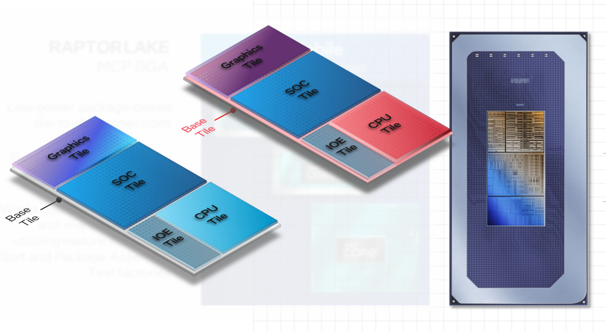
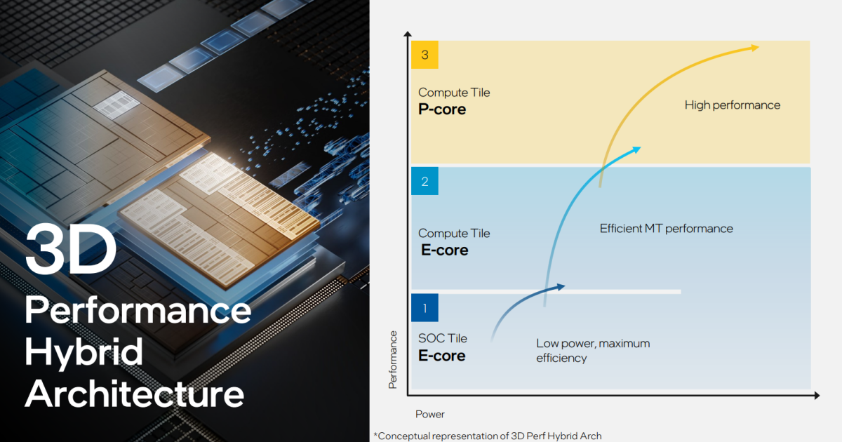
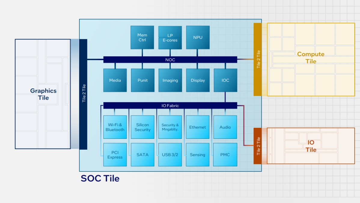
As you may count on, Intel’s new Meteor Lake is kind of sophisticated. Breaking it down into its element components, nevertheless, appears to take advantage of sense. Intel’s Meteor Lake has 4 tiles: one every for the CPU, the SOC, graphics, and I/O. We’ll clarify every in flip, digressing the place mandatory to clarify how Meteor Lake all suits collectively.
Intel
The street to Meteor Lake
Traditionally, an Intel CPU has been divided into two predominant components, packaged collectively: the CPU and Platform Control Hub, or PCH. A Direct Media Interface (DMI) bus linked the 2. In this scheme, it’s simple to consider the association because the CPU, and “everything else”: I/O, reminiscence, and so forth. (It’s not that clear-cut, however you get the thought.)
Intel’s new tiled association solves a number of issues. For one, every tile could be labored upon individually, by itself roadmap, and manufactured on the manufacturing course of it calls for. Intel makes use of its Foveros technology to attach and stack all of them collectively.
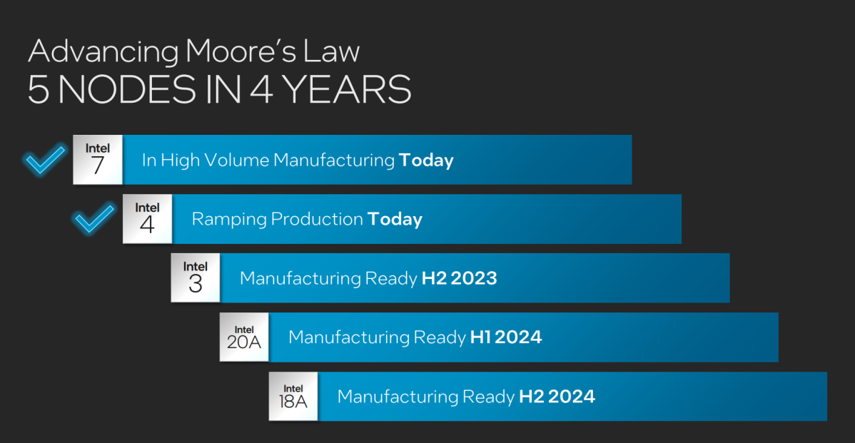
After stalling out on a 14nm manufacturing process for years, Intel’s new plan is to regain manufacturing management by striding by way of 5 new manufacturing course of applied sciences in 4 years, quicker than it ever has earlier than. But one of many promoting factors of Meteor Lake — that it’s an “Intel 4” chip — is a trifle misleading. Only the CPU tile is manufactured on Intel 4. In reality, the graphics tile and SOC tiles are fabricated at manufacturing rival TSMC.
Intel
Intel’s new tiles additionally imply that its logic could be intelligently separated from each other, saving energy. Each tile is linked by a material that gives roughly 128GB/s of bandwidth.
Intel’s chief govt Pat Gelsinger has referred to Meteor Lake as its “Centrino moment,” hearkening again to 20 years in the past when Intel launched the Centrino brand.
Centrino was the primary time that Intel bundled a CPU, chipset, and Wi-Fi chip collectively, however most neglect that it was additionally Intel’s response to Transmeta, a failed CPU startup that provided drastically decrease energy choices for laptops. Intel’s legacy CPU-PCH design meant that nearly all duties touched each chips, powering them up into an energetic state. Even although Intel then tried to return the CPU and PCH to a low-power sleep state as quickly as attainable, it nonetheless was an inefficient use of energy, Intel executives mentioned. By separating Meteor Lake into tiles, Intel can depart the unused tiles in a power-saving deep sleep mode.
According to Michelle Johnston Holthaus, govt vp and basic supervisor of Intel’s Client Computing Group, prospects requested for higher energy financial savings. Meteor Lake will ship the efficiency of Raptor Lake (or somewhat extra) at roughly half the facility, she mentioned.
“‘We love the performance that Intel delivers, but we want it in a more efficient power envelope and we want a more balanced platform,’” Holthaus advised PCWorld in an interview, referring to what she mentioned prospects have advised Intel. “This delivers all that.”
Intel
But there’s additionally an enormous secondary bonus, too: manufacturability. Intel’s Intel 4 course of is the primary to make use of Extreme Ultra Violet (EUV) lithography, a expertise that solves a elementary drawback: The transistors that Intel carves out of its photoresistive silicon wafers are smaller than the wavelengths of sunshine used within the etching course of. EUV (which requires a tough vacuum contained in the tools) is seen as the best way ahead to Intel 4 and past.
Intel doesn’t even manufacture all of its tiles itself. Intel’s Meteor Lake GPU tiles are made by TSMC, in its 5nm N5 course of; the SOC tiles are made by TSMC in its 6nm N6 course of, whereas the CPU tile is made by Intel on its Intel 4 course of. (Intel didn’t say who makes its I/O tile.)
Intel, led by CEO Pat Gelsinger, has pledged to roll out five process technologies in four years, believed to have begun with the Intel 7 course of utilized by the 12th-gen Alder Lake chips. The Intel 4 course of additionally makes use of an alloy known as enhanced copper, a mixture of copper and cobalt for superior conductivity, Bill Grimm, a vp in Intel’s Logic Technology Development group, mentioned.
Even higher, Grimm advised attendees that the smaller tiles additionally imply that they’re simpler to truly produce. Small errors within the manufacturing course of could make a chip too flawed to ship (an issue that the iGPU-less Intel “KF” sequence was designed to unravel). Smaller tiles additionally imply extra chips could be positioned on a wafer.
Intel
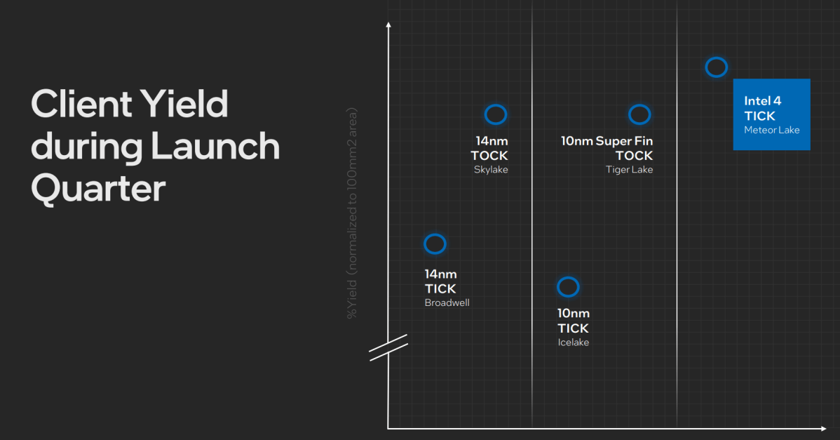
According to Grimm, Meteor Lake can be “the best yielding product at time zero [launch] in more than a decade.” Intel expects that Meteor Lake will see higher yields than both any 14nm or 10nm chips, he mentioned. That’s in all probability excellent news for the supply and worth at which Intel sells Meteor Lake to laptop computer makers.
Meteor Lake’s CPU tile
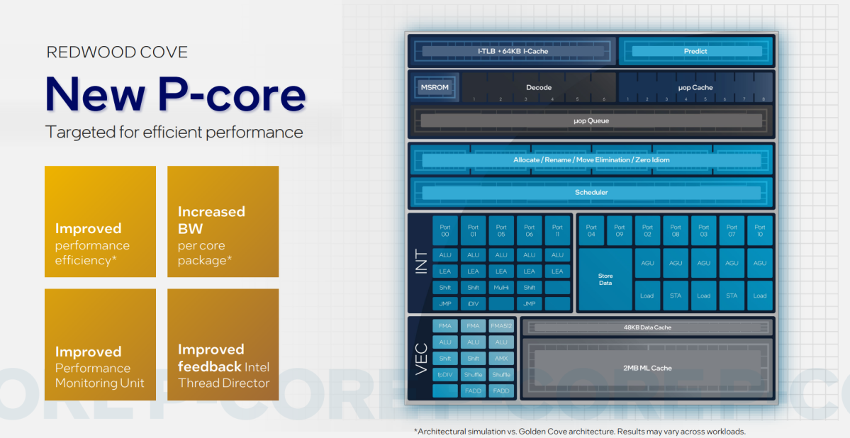
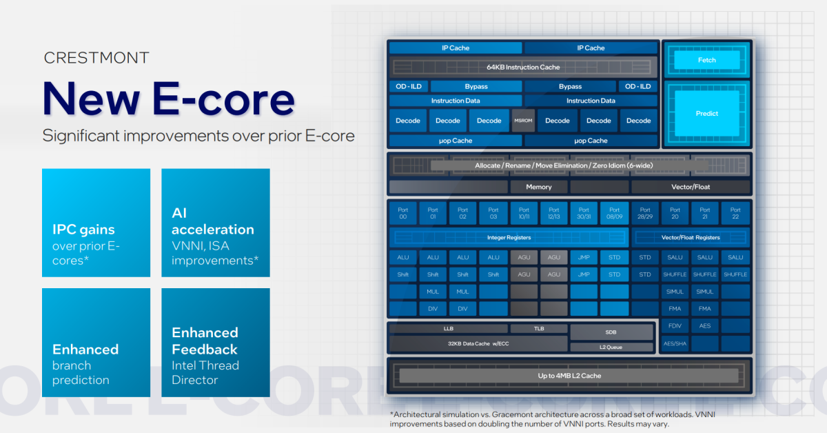
As with the 13th-gen Raptor Lake, Intel’s 14th-gen CPU tiles consists of two main components: the efficiency cores (P-cores), now often known as Redwood Cove, and the brand new effectivity cores (E-cores,) code-named Crestmont.
We actually don’t know that a lot about what variations there are between Raptor Lake’s P- and E-cores and people present in Meteor Lake. Redwood Cove, nevertheless, does provide improved efficiency effectivity and improved bandwidth, with a bigger, although undisclosed level-2 cache.
Intel
Intel additionally didn’t disclose something about Redwood Cove’s efficiency enhancements. Rajshree Chabukswar, an Intel fellow in its consumer programs and software program division, nevertheless, mentioned that Crestmont’s efficiency enhancements are between 4 to 6 p.c quicker when it comes to directions per clock versus Raptor Lake. (An IPC enchancment signifies that, if Raptor Lake and Meteor Lake had been to run on the similar pace, Meteor Lake’s Crestmont E-cores would run 4 to 6 p.c quicker.)
Intel isn’t revealing the varied Meteor Lake configurations, however it did exhibit one throughout its Tech Day presentation.
“For demonstration purposes during our Tech Day presentation, we showed a 6 [P-cores] +8 [E-cores] configuration,” an Intel spokesman confirmed in an e-mail. “However, we’ll be sharing additional product details closer to launch — including specifications, features, configurations, and performance data.”
Intel
To be honest, we don’t even formally know if Intel will ship a desktop model of Meteor Lake, which some name Meteor Lake-S. As for a rumored desktop “Rocket Lake Refresh” chip, Intel didn’t disclose that chip’s existence, both. We can hope that Intel provides some further clarifications this week at its Innovation convention.
Meteor Lake’s SOC tile: What low-power E-cores imply to you
One characteristic that’s not on the CPU tile are Meteor Lake’s new low-power E-Cores, and that was a deliberate alternative.
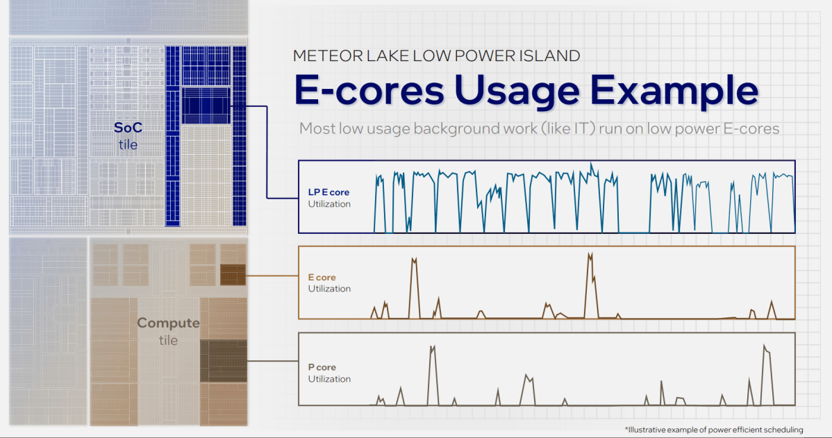
Meteor Lake’s two new low-power E-cores are contained inside the SOC tile, Meteor Lake’s most advanced when it comes to its array of capabilities. While the CPU tile accommodates the CPU cores, the SOC tile is basically the outdated PCH, housing the overwhelming majority of Meteor Lake’s secondary capabilities. Here, you’ll discover the low-power E-cores, the brand new NPU AI engine, in addition to the show engine, PCI Express, and extra.
Intel
Why put low-power E-cores right here? Again, that’s a part of Intel’s low-power plan: By separating the low-power E-cores from the CPU tile, that signifies that solely the SOC tile (or a particular portion of it) must be awoken into an energetic energy state. That saves energy, extending the laptop computer’s battery life.
So what’s a low-power E-core? Perhaps somewhat lamely, it’s a “new” E-core, a special model of the Gracemont structure. Recall that E-cores had been initially designed for low-power duties. The new low-power E-cores are designed for what executives known as background “IT tasks,” and it’s not clear what these are, solely. Nor do we all know how “low power” these new cores are.
One moderately stunning instance of what these “IT tasks” entail, nevertheless, was when Intel executives used a low-power E-core to play again Tears of Steel, the open-source video file that we use to measure a laptop computer’s battery life. That’s spectacular!
Historically, taking part in again video demanded the eye of all the CPU up till about 2017. Then, in Lakefield and Alder Lake, Intel started assigning that activity to E-cores and P-cores. Now, video playback has migrated to a tiny portion of Meteor Lake. Imagine how usually you play again video. The battery lifetime of laptops ought to enhance dramatically simply primarily based upon this activity alone.
Intel
Meteor Lake’s Thread Director makes energy, not efficiency, the precedence
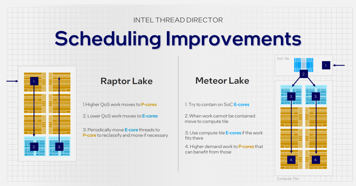
Intel has additionally massively altered Thread Director, the mechanism by which threads or workloads are shunted between cores, inside Meteor Lake. Windows or Linux understands what must be accomplished and instructs the CPU to take over. That job is then handed to Thread Director. In Thread Director 2, working on the Core i9-13900Ok, duties had been routed to the efficiency cores first, then shunted to the E-cores if wanted.
In Meteor Lake, it’s the reverse: Threads are first assigned to the low-power E-cores, then the full-power E-cores, and lastly to the P-cores. Thread Director assigns duties totally different priorities after which assigns the duties accordingly. (The duties are rated not on their efficiency, however by different traits: “0” is “idle,” “2” is “sustained,” and “3” is “bursty.”)
And Intel is severe about this: If a low-power E-core finishes a activity and is freed up, an obtainable thread can be pushed to it, even when a P-core is out there, Chabukswar mentioned. Even in a state of affairs the place a P-core is free, and Intel’s Thread Director is optimized for efficiency (maybe through the Windows power slider), duties can be assigned to the E-cores first, she mentioned.
Intel
We’ve gone down this street earlier than. Though Intel seems to have the ability to alter Thread Director as a coverage, we don’t know whether or not it can. Could a gaming-optimized laptop computer characteristic predominantly P-cores, with Thread Director routing threads to the P-cores first?
Chabukswar agreed that Thread Director might be adjusted for the wants of gaming. What isn’t solely clear is whether or not there can be a efficiency penalty for beginning a gaming thread, for instance, on a low-power E-core, then stepping it by way of to an E-core after which to a P-core — moderately than recognizing that it wanted a P-core to start with.
Intel already disclosed a few of its power-management plans earlier than at this time. At the Hot Chips convention in August, Intel disclosed that it would use “AI” on Meteor Lake to find out how a person interacts with a typical activity like opening an internet web page.
By shortly shifting threads to the correct cores after which dropping into an idle state, Intel believed it may save 10 to 20 p.c in power with out impacting the person expertise. But Meteor Lake gained’t study from you: Instead, Intel is taking a median of kinds from what the machine-learning algorithm has discovered from its check customers.
Intel executives additionally disclosed that they’re working carefully with Microsoft, in order that fundamental Windows capabilities could be assigned to the correct cores.
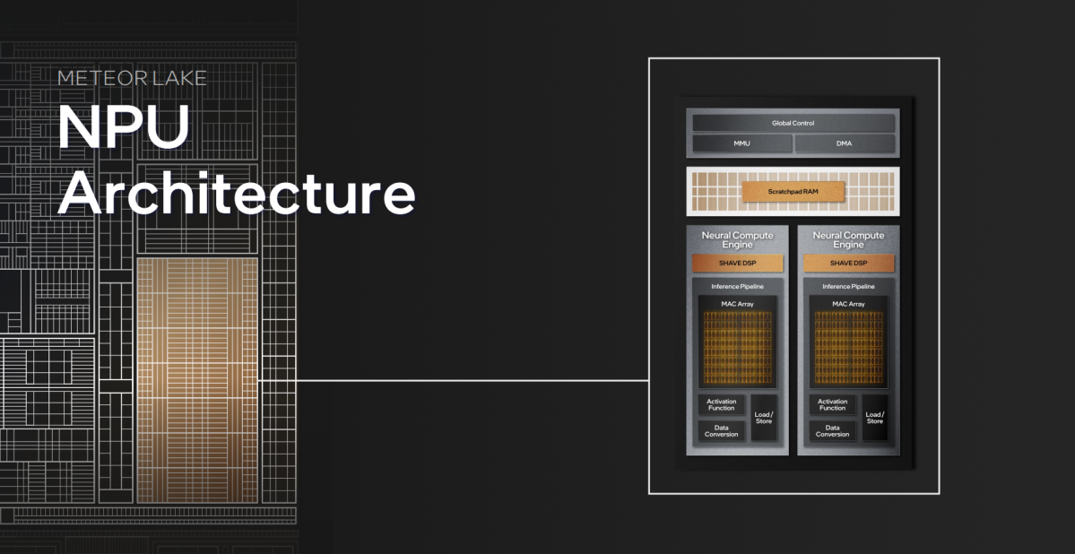
Meteor Lake’s SOC tile: AI arrives in your PC through the NPU
The SOC tile can be residence to what Intel calls the NPU, or AI block. In 2022, Intel CEO Gelsinger confirmed that AI was coming to Meteor Lake, launching the “AI PC era.” According to Holthaus, Intel will ship “millions” of those AI PCs. Incidentally, this NPU can be on all variations of Meteor Lake, Intel confirmed.
Intel
Intel is definitely on its third technology of AI: The first technology it bought from Movidius in 2016, later constructing discrete playing cards into some PCs just like the Samsung Galaxy Book3 Ultra that allow these PCs to do background blurring and noise filtering through what’s often known as Windows Studio Effects. (While Windows Studio Effects use the Movidius expertise, Zoom, Teams, Google Meet, and others merely use your PC’s CPU or GPU as a substitute.)
What Intel is attempting to do is place the PC for future AI purposes, even when it doesn’t know precisely what they’ll be. Tom Petersen, an Intel fellow, confirmed off Stable Diffusion, an AI artwork generator. He additionally demonstrated a plugin for audio editor Audacity that not solely separated the vocals from the backing devices, however later altered that instrumental fashion utilizing a textual content immediate. Intel’s objective seems to be the tide that lifts all boats, accelerating AI APIs like WinML, DirectML, and its personal OpenVINO inference engine.
“Our goal is to democratize AI,” mentioned Tim Olson, basic supervisor of SOC design for Intel, in a separate presentation.
Intel
The NPU is one a part of that. Intel’s NPU features a pair of neural compute engines, every with two VLIW Shade DSPs inside, with inference engines able to as much as eight directions per cycle. Even for customers used to parsing the variety of cores per chip, base clocks, and turbo clocks, this gained’t make lots of sense. What Intel is attempting to convey is that AI requires a ton of multiply-accumulate (MAC) directions per cycle, and that these engines can carry out 2,048 MAC calculations every.
Is that good? Is that dangerous? We actually don’t know. We don’t actually have a basic level of reference for what makes for “good” AI, when it comes to specs or benchmarks, and Intel executives gave us the concept they’re attempting to work that out, too.
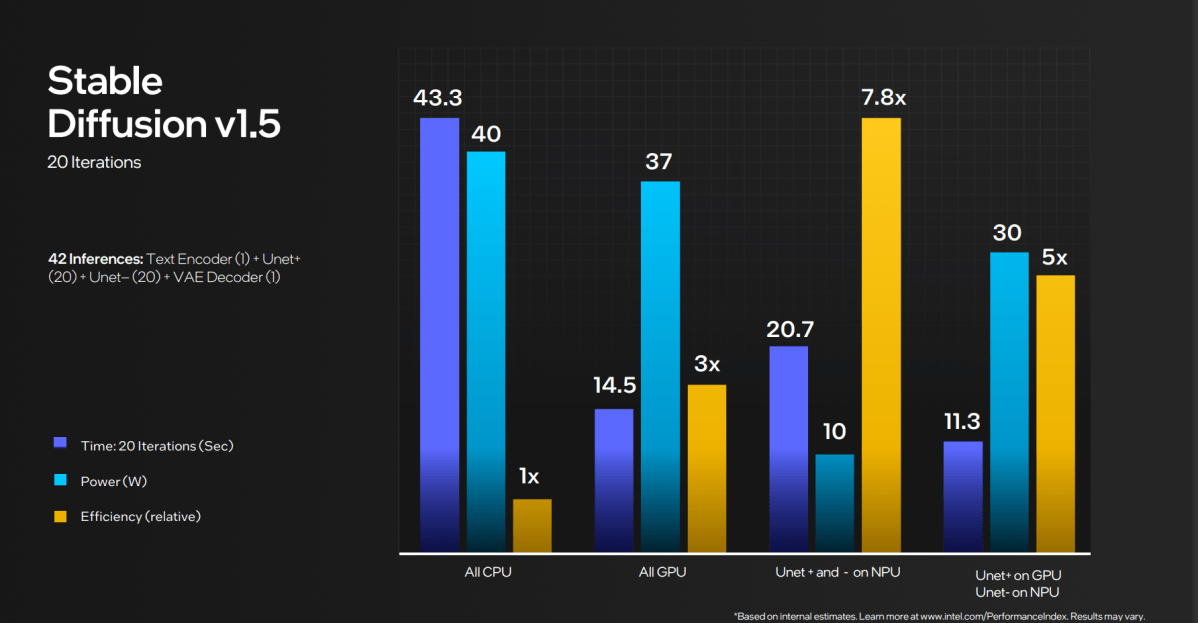
Intel’s secret sauce, although, isn’t simply the AI NPU, however how the CPU, GPU, and NPU can all assist help one another. Take the next instance. Running 20 iterations of Stable Diffusion, Intel tried numerous combos: performing all the calculations on the CPU, all on the GPU, all on the NPU, and a mixture of all three. Performing all of them on the NPU took 20.7 seconds and 10 whole watts, probably the most environment friendly use. But performing all of them on the GPU and NPU completed the duty in 11.3 seconds, consuming 30W.
Which is best? Ideally, the person and/or Windows will make that call. But it’s not a simple, easy answer.
Intel
Intel can be integrating what it calls the DP4A instruction into the GPU, a GPU instruction particularly designed to speed up AI.
Remember, Intel’s not disclosing all of what Meteor Lake hides. We know, for instance, that PCI Express Gen 5 (PCIe 5) can be supported, however not what number of lanes. Ditto for what taste of Ethernet the chip will assist, or the variety of USB bus connections. It seems, although, that the chip will assist Thunderbolt 4, however not the upcoming 80Gbps model, Thunderbolt 5.
Intel executives additionally mentioned that the chip would assist DDR5 and LPDDR5, however we don’t know for sure if that excludes DDR4 or LPDDR4. Intel has confirmed that each Wi-Fi 6e and Wi-Fi 7 can be supported, nevertheless, giving gobs of headroom for persistent wi-fi connectivity.
Intel basically separated the SOC tile into two halves, with an I/O cloth connecting all the I/O (Ethernet, Wi-Fi, and so forth) to the I/O tile. A separate NOC cloth connects the low-power E-cores, NPU, and show controller. (A small I/O controller connects each halves.) Again, this was accomplished to reduce energy consumption, as every half can work as independently as attainable.
Intel’s imaging and show blocks assist HDMI 2.1, DisplayPort 2.1, and embedded DisplayPort 1.4. One vital characteristic that Intel is disclosing is what number of shows Meteor Lake will assist: as much as a single 8K60 show (with HDR), or 4 4K60 shows, once more with HDR. And if you happen to’re a gamer, Meteor Lake will assist a single 1080p or 1440p show at 360Hz. That’s a giant deal.
Intel
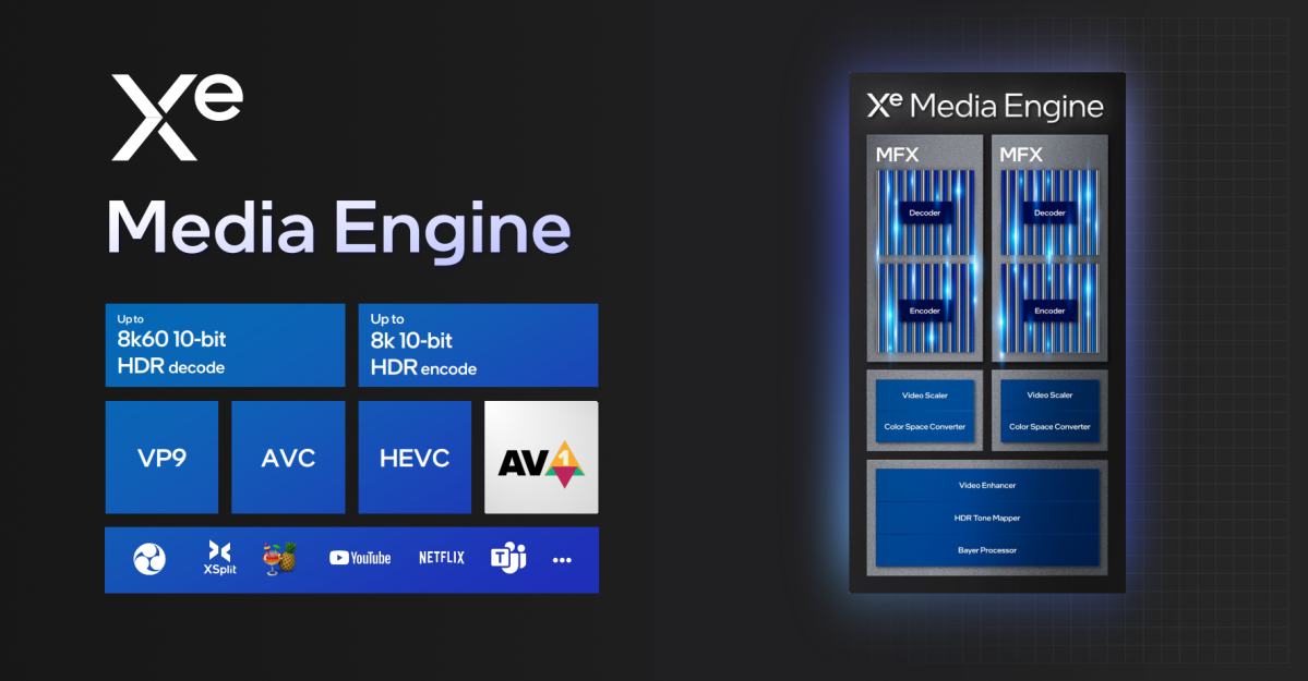
The media engine will assist 8K60 10-bit HDR decode and encode, with assist for numerous codecs. Among them is the open-source AV1 codec, which has already demonstrated impressive encoding results running under Intel’s standalone Arc chip.
Intel additionally put a small twist in its show engine to save lots of energy: If the identical body occurs to repeat, Meteor Lake is wise sufficient that it may depart the body off solely. Two of its 4 show pipelines are additionally optimized for low energy, which Petersen highlighted as a possible answer for a digital keyboard on a foldable gadget.
Meteor Lake’s graphics tile: Ray tracing in an built-in GPU?
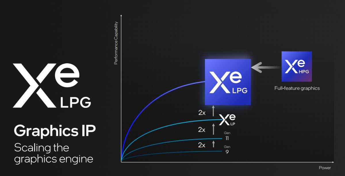
While Intel’s debut in the PC graphics space offered a welcome third competitor, the corporate’s efforts in each the built-in and discrete graphics market have had their points. Meteor Lake and what Intel calls its XeLPG graphics block mix components of each markets, updating the Xe (or XeLP) built-in GPU that has been inside Core processors for the previous few years. Essentially, Intel is taking as a lot as it may from its standalone Arc GPUs and placing it contained in the built-in Meteor Lake GPU.
“We’ve taken all the goodness from our XeHPG architecture and put it into our XeLPG architecture,” Petersen mentioned. Even higher, by inserting graphics on a separate tile, Intel can combine and match graphics efficiency for the promote it’s pursuing, Petersen added.
Intel
According to Intel’s Petersen, Intel is concentrating on twice the efficiency of the sooner Xe core, and twice the efficiency per watt, too. Intel is rising the XeLPG’s clock speeds, dedicating extra silicon to it, and making it extra environment friendly.
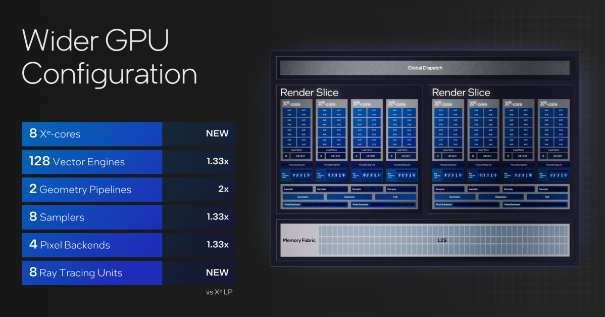
Finally, Intel is bringing within the eight Xe cores from the Arc A770 in addition to eight ray-tracing items into Meteor Lake. Yes, which means ray tracing is now a part of the fundamental built-in GPU, and never only a discrete chip. Petersen did admit, nevertheless, that it will be as much as software program builders to take benefit.
Intel
Put merely, evaluate our earlier deep dive into the XeHPG architecture and all of it seems to be extraordinarily related: Inside every “slice” of the XeLPG core are 4 Xe cores, with 16 256-bit vector engines and 192KB shared L1/SLM cache. Intel helps DirectX 12 Ultimate natively.
There are new bits, too. The new structure helps FP64 directions — Arc doesn’t — plus out-of-order sampling, and Intel’s software program companions advised Intel that together with FP64 would do wonders for software program compatibility, Petersen mentioned.
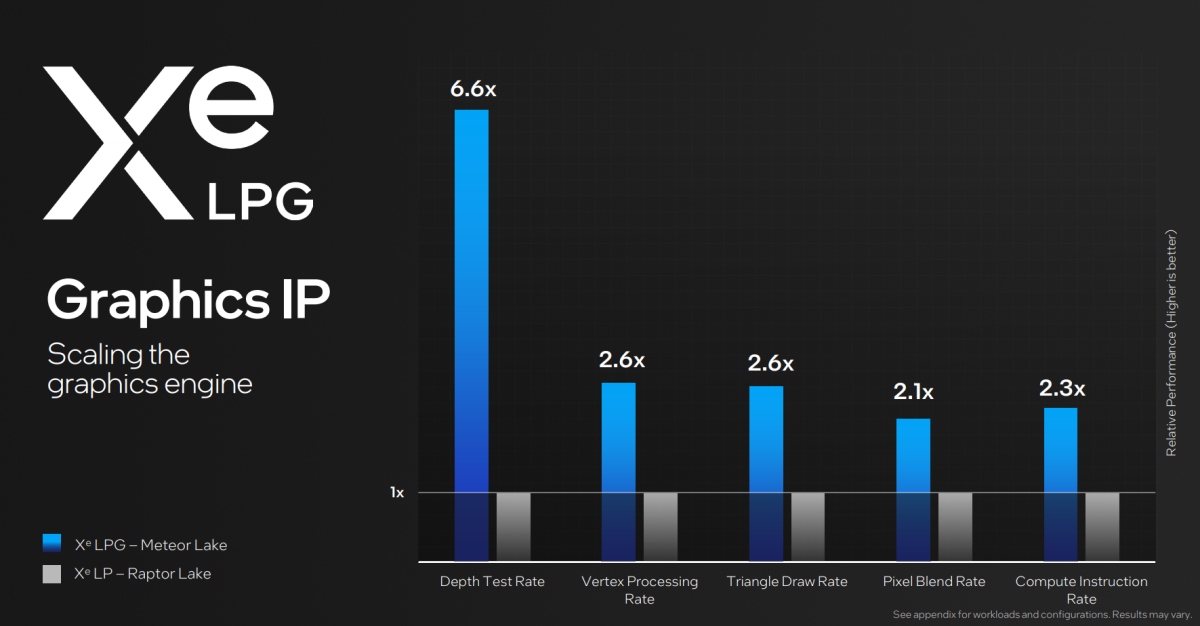
While Intel declined to share precise sport efficiency knowledge, Petersen did conform to share a few of its “micros,” or inside summary efficiency checks. Measurements starting from triangle draw price (2.6X over the XeLP present in Raptor Lake) to depth check price (6.6 instances Raptor Lake) are one indication that Intel believes that its new Xe cores are head and shoulders above its older expertise. Intel additionally confirmed off Forza Horizon 5 working on the Meteor Lake {hardware}, however didn’t disclose the decision or graphics settings.
Intel
Meteor Lake’s XeLPG additionally helps XeSS, Intel’s reply to Nvidia’s DLSS. Intel’s expertise renders the body at a decrease decision, then supersamples it as much as a high-res picture.
According to Petersen, this protects power in addition to improves the picture; making use of XeSS lowers the power consumed to 526 millijoules versus 863 millijoules. Meanwhile, Peterson confirmed off body charges that elevated to 1.69X or so when XeSS was turned on.
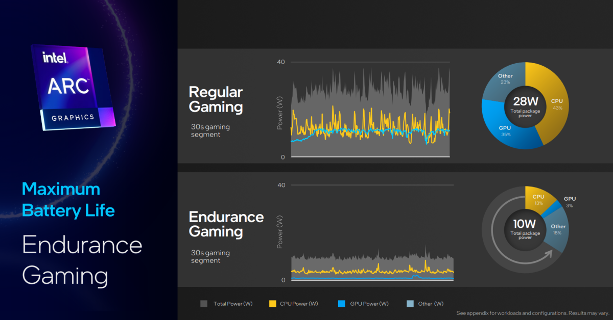
Finally, Meteor Lake introduces what Intel calls Endurance Gaming, which can use the Intel Arc Control utility for energy administration. The app talks on to Intel’s cell drivers, moderating efficiency and enhancing effectivity; in a “regular gaming” mode, Arc Control, may allocate 28W to all the system, together with the CPU and GPU. In Endurance Gaming, that might be lower to a complete of 10W, giving simply 1W to the CPU. Intel’s Petersen mentioned that the sport Rocket League might be run at 30 frames per second at lower than 1W of energy.
Intel
Appendix: Meteor Lake’s I/O tile
We’re not going to speak in regards to the fourth I/O tile, exactly as a result of Intel barely touched upon it. With a lot of the “I/O” capabilities truly contained inside the SOC tile, a number of the further, market-specific performance might reside right here. What that can be, and what it can appear to be, isn’t actually recognized.
Intel confirmed that Meteor Lake could have Thunderbolt 4, not 5, connectivity to external Thunderbolt docks, in addition to exterior USB performance — no surprises there. But Intel fellow Mikal Hunsaker additionally indicated that the I/O tile is also reworked to satisfy the wants of the market.
One query that leaves us with: How shortly will every of those tiles be overhauled? We can’t assist however assume somewhat of how Windows apps like Photos at the moment are on their very own improvement cycle, and never tied to any explicit Windows launch. It looks like Intel might undertake an identical method.
Intel’s system-level applied sciences
Intel, naturally, doesn’t simply manufacture PC silicon — its Arc software program is proof of that. But Intel additionally outlined a number of the system-level initiatives it will concentrate on with Meteor Lake platforms, too:
Wi-Fi 7: Intel’s BE200 radio chip (aka Gale Peak 2) can be used alongside Meteor Lake platforms. It helps Bluetooth LE with decrease energy and latency, in addition to Wi-Fi 7 — with speeds of as much as 5.76Gbps, it’s theoretically quicker than most implementations of wired Ethernet.
Intel Unison: Intel’s Unison software program is like Windows’ personal Your Phone, however it’s the best solution to get the iPhone’s iMessage communication in your PC. It’s far more highly effective with Android, although, and the up to date Unison software program will assist extending your laptop computer’s display onto an (Android) pill, in addition to more practical wi-fi communication that may reap the benefits of a number of wi-fi connections.
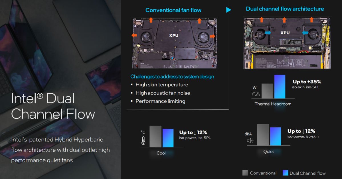
Intel Cool, Quiet, Performant: Part of Intel’s Evo program is working with PC makers to assist co-engineer their notebooks and desktops. Intel confirmed off its dual-channel hyberbaric circulate design that it patented, and can be utilized with laptops. It additionally developed an ultrathin vapor channel, additionally patented, that it may provide to pocket book makers. Specific software program to optimize fan pace and analyze workloads to shift efficiency up and down are additionally choices.
Intel
The fan speeds controls had been designed with acoustics in thoughts, so that they’ll scale up slightly below the purpose the place you’ll discover the fan noise annoying. The workload evaluation software program seems to be, or be associated to, the AI-powered power-management techniques Intel confirmed off beforehand at Hot Chips.
Conclusion
Intel might have offered us a large quantity of details about its Meteor Lake chip, however we nonetheless don’t know that a lot in regards to the 14th-gen Core: when precisely it can ship, its clock speeds, how it will likely be configured for its numerous markets, and so forth. Interestingly, Intel has splintered its Xeon server chip roadmap into two totally different forks: Sierra Forest, made up of all E-cores, and Granite Rapids, consisting of all P-cores. Intel’s tiled structure ought to enable it a few of these choices, if it so chooses.
We nonetheless await AMD’s response within the pocket book house, and even Qualcomm’s reply with its Oryon (Nuvia) technology. But Intel nonetheless ships the overwhelming majority of all laptop computer CPUs, making it the dominant participant within the house. You’ve possible simply learn the precise particulars of your subsequent laptop computer’s microprocessor.
Updated at 9:23 AM on Sept. 19 with further particulars.